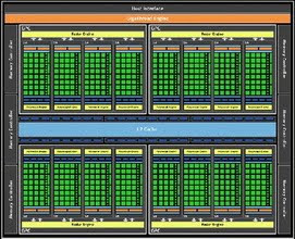
Vendor chip maker, Nvidia has released details of the Fermi Graphics graphics processor 100 (GF100), which was delayed, which has 384-bit memory interface. GPU (graphics processing unit) of new generation will be equipped with 3 billion transistors and 512-core CUDA, Nvidia will also integrate parallel computing capabilities and performance for applications including pehitungan physics, higher mathematics calculation, linear algebra and the search algorithm.
Nvidia to make CUDA-based Fermi architecture, which facilitates the Nvidia GPU executes programs written in C, C + +, Fortran, OpenGL, DirectCompute, and other languages. With this core CUDA 512, arranged in 16 SMS (stream processors) in each of 32 cores. GF100 Nvidia GPU has 64-bit memory partitions, and support 6GB memory GDDR5 DRAM. GPU interface to be connected to the CPU via the PCI-Express, and each BC will have a processor 32 CUDA. Each processor is equipped CUDA ALU (arithmetic logic unit) integer and floating point unit (FPU).
Fermi also support the execution of different kernels in which the kernel can execute the same applications and at the same time. Facilitate the execution of the kernel to execute a program that small kernel to move the whole GPU. In Fermi GF100 chip architecture, the kernel is different in the same CUDA context may use the maximum utilization of GPU resources.
This time, Nvidia has not revealed other important information about the GF100, such as manufacturing processes, clock speed, performance, power usage, and price.

0 komentar:
Posting Komentar